Electric Field Optimization
- Electric field optimization in optical multilayers is a key feature for a range of applications. In high‑power laser systems, high peak electric‑field intensity can lead to damage in multilayer coatings. By tailoring the design to shift field maxima into low‑index layers or away from high/low‑index interfaces, the damage threshold can be increased.
- OTF Studio provides a special type of design targets, E‑Field targets, which enable inclusion of electric‑field optimization into the coating synthesis process. The E‑Field targets can be flexibly specified. Target parameters include:
- polarization,
- incidence angle,
- wavelength range,
- the layer material in which the electric field should be optimized,
- the Goal, and
- the Goal Region (boundary or center).
- As a Goal two options are offered: Min (minimize the electric field in the selected region) and Max (maximize the electric field in the selected region).
- Goal Region specifies the part of the layer where the optimization is applied: Boundary near the layer interfaces, or Center around the central portion of the layers (Fig. 1).
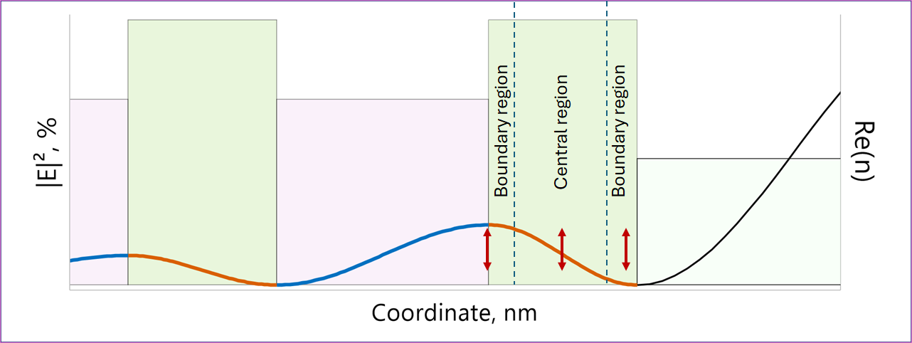
Fig. 1. Goal regions for specification of the electric‑field target: Boundary and Central.
- Typical applications for laser‑related coatings involve suppression of the electric field near layer interfaces in high‑index materials and shifting electric‑field maxima into low‑index layers.
- Typical applications for coatings used in optical sensors involve enhancement of the electric field within the coating structure.
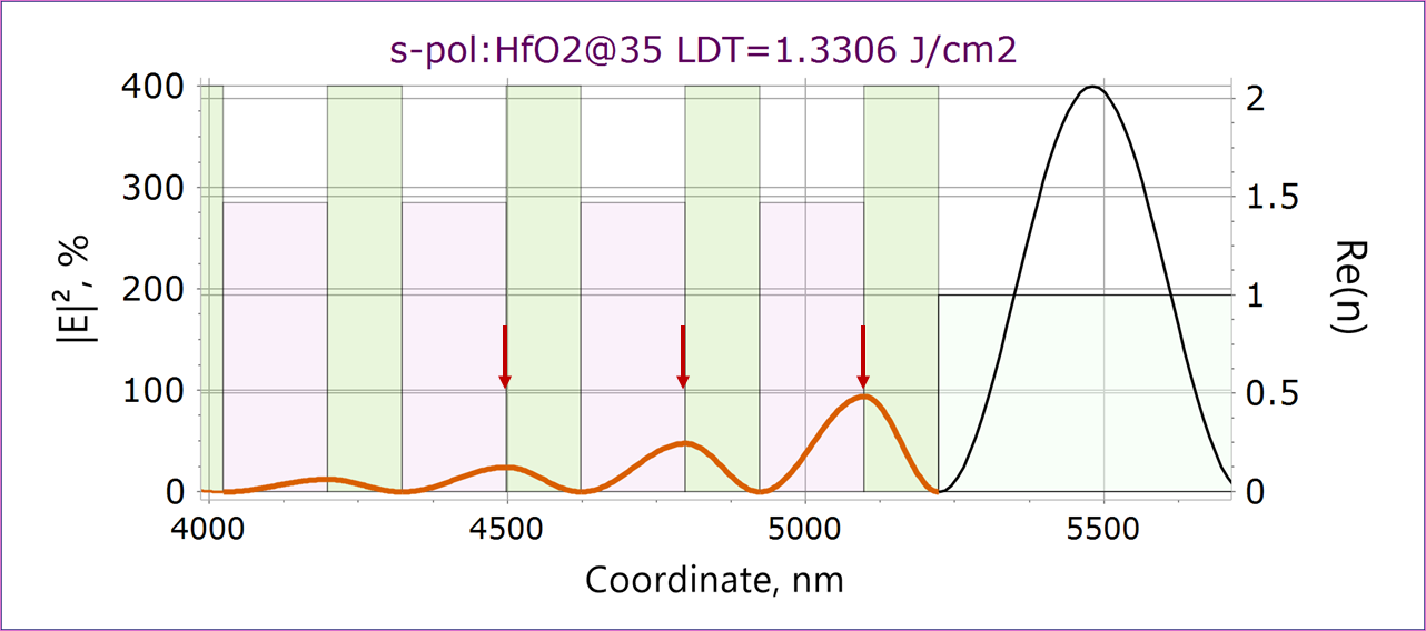
Fig. 2. Electric field distribution of a 35-layer HfO2/SiO2 quarter-wave mirror at the central wavelength of 1030 nm.
- Fig. 2 shows the electric‑field distribution of a 35‑layer HfO₂/SiO₂ quarter‑wave mirror at the laser wavelength of 1030 nm. The mirror structure and its spectral reflectance are shown in Fig. 3.
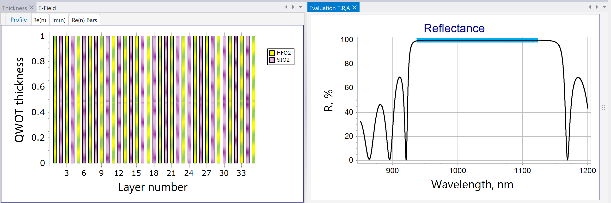
Fig. 3. Structure (left) and reflectance (right) of a 35-layer HfO2/SiO2 quarter-wave mirror at the central wavelength of 1030 nm.
- The E‑Field target in OTF Studio was formulated to suppress electric‑field maxima in the HfO₂ layers. This target was applied together with the high‑reflectance target (markers in Fig. 3) to maintain high reflectance of the multilayer around the central wavelength.
- The resulting high reflector, with electric‑field distribution shown in Fig. 4, is expected to have a higher damage threshold than the initial quarter‑wave mirror design.
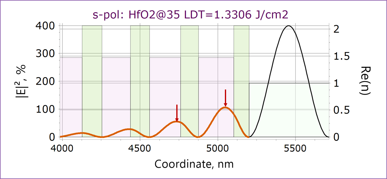
Fig. 4. Electric field distribution of the optimized 35-layer HfO2/SiO2 multilayer design (Fig. 5) at the central wavelength of 1030 nm.
- OTF Studio displays the LDT estimation on the E‑Field plot if intrinsic values of layer materials are known and specified. The layer material and the layer number with the maximum LDT are also shown. The LDT estimation is performed using formulas from Ref. [1]. The optimized design shows a higher LDT value than the initial quarter‑wave design.
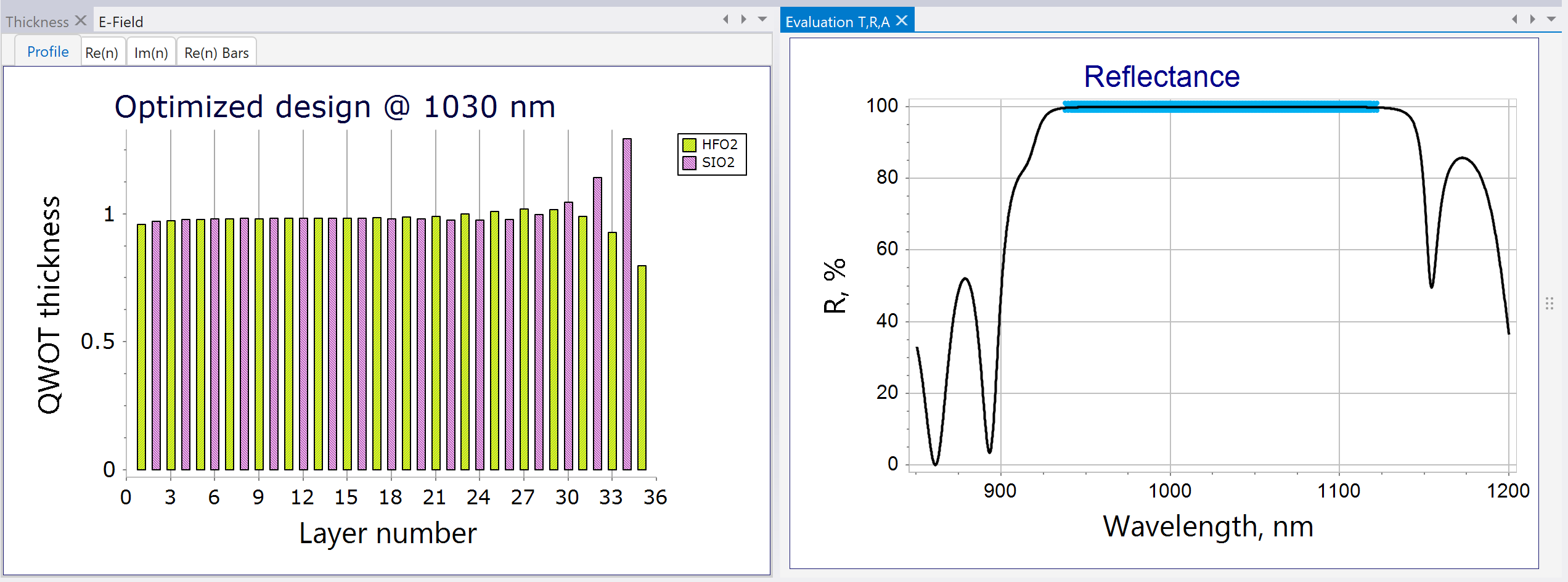
Fig. 5. Structure (left) and reflectance (right) of the optimized 35-layer HfO2/SiO2 multilayer at the central wavelength of 1030 nm.
[1] A. Hervy, et al., “Femtosecond laser-induced damage threshold of electron beam deposited dielectrics for 1-m class optics,” Opt. Eng. 56 (1), 011001 (2016). https://doi.org/10.1117/1.OE.56.1.011001
-
For trial versions, please contact our authorized distribution partners according to your region.